产品介绍

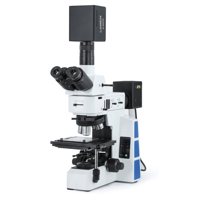
Function of camera:
1. with standard C interface imaging lens or directly integrated with the microscope, spectral imaging (Mapping) rapid acquisition
2. ae, automatic scanning speed matching, automatic acquisition and save the data
3. data real-time calibration and model operation function can be realized
4. auxiliary view camera for shooting area monitoring
5. built-in battery
6.data preview and correction function: radiometric correction and reflectance correction uniformity, regional correction, camera calibration, the calibration
7.lens can be replaced
8.data format compatible with En-vi, perfect Spec-Sight data analysis software, etc
9.target spectral matching real-time search function
10 built-in WiFi support Android smartphone, tablet, i-phone wireless remote control
11.gigabit Ethernet: support for remote image transmission and remote control
Biomedical domain:
As a non-invasive method for diagnosis and evaluation of treatment, HSI has a wide range of potential uses in the biomedical field. HSI has the ability to extract spectral features of each pixel from hyper-spectral images while providing information about different tissue components and their spatial distribution. Under specific wavelength, the chemical composition and physical characteristics of tissues with different pathological states have different absorbance and reflectance, which is reflected in the difference of characteristic spectra. By analyzing these spectral signals, the qualitative or quantitative detection of tissue state information can be realized, and the visual diagnosis of pathological states of different tissues can be realized. For example, the micro-hyper-spectral imaging system can be used for the identification of tumor cells, the identification of hemorrhagic polyps, the identification of meat leukaemia, the screening of lymphocytic leukemia, the differentiation of cytoplasm and nucleus, and the calculation of cell number.

FIG. 4 Rapid identification of laryngeal mucosal hemorrhagic polyps and meat day shift area based on microscopic hyper-spectroscopy (red area)

FIG. 5 Microscopic hyper-spectral identification of tumor location and abnormal cell diffusion location under 20X eyepiece

Figure 6 Rapid differentiation of nuclei, cytoplasm and other substances based on microscopic hyper-spectroscopy

FIG. 7 Cell number calculated according to the location of cell barycenter
Detection of dark field scattering nanometer particles
Dark field microscopy is a special microscopic method realized under dark field illumination, which can avoid the light unrelated to the object being observed from entering the objective lens and present a clear object outline in the dark background. The spatial resolution of this method is 50 times higher than that of ordinary open-field lighting microscopy, which is enough to observe the tiny particles at 4~200nm. Microscopes equipped with hyper-spectral imaging system can distinguish the species and spatial distribution of particles by spectral characteristics. At right, VNIR hyper-spectral imaging of lung tissues from mice was performed after a single intratracheal infusion of low (18 pg) and high (162 pg) doses of nanometer titanium dioxide to determine particle retention in these tissues.

Figure 8 Dark-field image of tissue exposed to nano-tiO2 (top); Dark-field hyper-spectral images from tissue exposed to nano-tiO2 identified these nanometer particles, which appeared as aggregates of white inclusions (middle image); nanometer titanium dioxide in these tissues appears as red dots or aggregates in hyper-spectral images (bottom)
Luminescence test of OLED display:
The micro-hyper-spectral imaging system can obtain the luminous images of OLED display with higher spatial resolution through eyepieces of different multiples, and detect the luminous uniformity and stability of OLED display through the feature of "atlas integration" of hyper-spectral image data.

Chip material, defect detection:
The PL Mapping of the entire wafer can be obtained by using micro-hyper-spectral imaging technology, which is a non-contact, non-damaging, fast and accurate micro-zone measurement technology, which can be operated at room temperature or can be measured online in production, so as to obtain important information about the composition ratio of substrate or epilayer, defects and micro-zone uniformity of other properties of the material. The micro-hyper-spectral imaging technique can be used to identify the texture of the wafer and the variation of the luminescent center concentration of the sample on a fine scale.

FIG. 10 Microscopic hyper-spectral imaging images and spectra of chips implanted with boron, aluminum and without special materials
Application of perovskite crystals:
In recent years, the continuous discovery of sensitive, cheap and easy to process photovoltaic materials has promoted the rapid development of organic perovskite solar cells. Their high carrier mobility and strong absorbance with tun-able band gaps in the visible light range make them ideal for the production of low-cost solar panels. However, due to the poor stability of these materials, more convenient and effective techniques are urgently needed to help people better understand the physic-chemical mechanism of their photovoltaic degradation.
Compared with traditional detection techniques such as confocal microscopy, micro hyper-spectral imaging has the following advantages in detecting the inhomogeneity of crystal materials: the excited light intensity is uniformly distributed in the entire field of view, and the spectral information of the entire field of view can be obtained by a single imaging, and the quantitative value of spectral intensity can be obtained.

Figure 11 shows PL data for perovskite
Figures (a) and (b) show two different monochromatic PL images taken at 625 nm and 750 nm, respectively. Figure (c) shows the spectral images of different positions in Figure 1, and Figure (d) shows the frequency shift imaging images of PL maps in the specified region
Application on LED/OLED light source display:
With the progress of photoelectronic technology, the requirements for semiconductor product testing are increasing day by day. Single point spectral testing is difficult to meet the requirements. Micro-hyper-spectral imaging technology is gradually applied in the testing field of semiconductor materials and devices. At present, micro-hyper-spectral imaging technology is mainly used in the study of luminescence uniformity of semiconductor materials, detection and analysis of semiconductor material defects, detection and inversion of the surface temperature spatial distribution of LED chips, etc.

Figure 12 Microscopic hyper-spectral inversion of the temperature of different LED light source panels
应用领域
1、生物医学领域
2、暗场散射纳米颗粒检测
3、OLED显示屏发光测试
4、晶片材料
5、缺陷检测
6、钙钛矿晶体中的应用
7、LED/OLED光源显示屏上的应用
文档下载